
3.3.1 General discussion - Poisson's equation |   |
The electrostatic analysis of a metal-semiconductor junction is of interest since it provides knowledge about the charge and field in the depletion region. It is also required to obtain the capacitance-voltage characteristics of the diode. |
The general analysis starts by setting up Poisson's equation: |
| (3.3.1) |
Where the charge density, ρ, is written as a function of the electron density, the hole density and the donor and acceptor densities. To solve the equation, we have to express the electron and hole density, n and p, as a function of the potential, φ, yielding: |
| (3.3.2) |
with |
| (3.3.3) |
where the potential is chosen to be zero in the n-type region, where x >> xn. |
This second-order non-linear differential equation (3.3.2) cannot be solved analytically. Instead we will make the simplifying assumption that the depletion region is fully depleted and that the adjacent neutral regions contain no charge. This full depletion approximation is the topic of section 3.3.2. |
3.3.2 Full depletion approximation | |
The simple analytic model of the metal-semiconductor junction is based on the full depletion approximation. This approximation is obtained by assuming that the semiconductor is fully depleted over a distance xd, called the depletion region. While this assumption does not provide an accurate charge distribution, it does provide very reasonable approximate expressions for the electric field and potential throughout the semiconductor. These are derived in section 3.3.3. |
3.3.3 Full depletion analysis | |
We now apply the full depletion approximation to an M-S junction containing an n-type semiconductor. We define the depletion region to be between the metal-semiconductor interface (x = 0) and the edge of the depletion region (x = xd). The depletion layer width, xd, is unknown at this point but will later be expressed as a function of the applied voltage. |
To find the depletion layer width, we start with the charge density in the semiconductor and calculate the electric field and the potential across the semiconductor as a function of the depletion layer width. We then solve for the depletion layer width by requiring the potential across the semiconductor to equal the difference between the built-in potential and the applied voltage, φi - Va. The different steps of the analysis are illustrated by Figure 3.3.1. |
As the semiconductor is depleted of mobile carriers within the depletion region, the charge density in that region is due to the ionized donors. Outside the depletion region, the semiconductor is assumed neutral. This yields the following expressions for the charge density, ρ: |
| (3.3.4) |
where we assumed full ionization so that the ionized donor density equals the donor density, Nd. This charge density is shown in Figure 3.3.1 (a). The charge in the semiconductor is exactly balanced by the charge in the metal, QM, so that no electric field exists except around the metal-semiconductor interface. |
| Figure 3.3.1 : | (a) Charge density, (b) electric field, (c) potential and (d) energy as obtained with the full depletion analysis. |
Using Gauss's law we obtain the electric field as a function of position, also shown in Figure 3.3.1 (b): |
| (3.3.5) |
where εs is the dielectric constant of the semiconductor. We also assumed that the electric field is zero outside the depletion region, since a non-zero field would cause the mobile carriers to redistribute until there is no field. The depletion region does not contain mobile carriers so that there can be an electric field. The largest (absolute) value of the electric field is obtained at the interface and is given by: |
| (3.3.6) |
where the electric field was also related to the total charge (per unit area), Qd, in the depletion layer. Since the electric field is minus the gradient of the potential, one obtains the potential by integrating the expression for the electric field, yielding: |
| (3.3.7) |
We now assume that the potential across the metal can be neglected. Since the density of free carriers is very high in a metal, the thickness of the charge layer in the metal is very thin. Therefore, the potential across the metal is several orders of magnitude smaller than that across the semiconductor, even though the total amount of charge is the same in both regions. |
The total potential difference across the semiconductor equals the built-in potential, φi,in thermal equilibrium and is further reduced/increased by the applied voltage when a positive/negative voltage is applied to the metal as described by equation (3.2.5). This boundary condition provides the following relation between the semiconductor potential at the surface, the applied voltage and the depletion layer width: |
| (3.3.8) |
Solving this expression for the depletion layer width, xd, yields: |
| (3.3.9) |
3.3.4. Junction capacitance | |
In addition, we can obtain the capacitance as a function of the applied voltage by taking the derivative of the charge with respect to the applied voltage yielding: |
| (3.3.10) |
The last term in the equation indicates that the expression of a parallel plate capacitor still applies. This can be explained by the fact that the charge added/removed from the depletion layer as one decreases/increases the applied voltage is added/removed only at the edge of the depletion region. While the parallel plate capacitor expression seems to imply that the capacitance is constant, the metal-semiconductor junction capacitance is not constant since the depletion layer width, xd, varies with the applied voltage. |
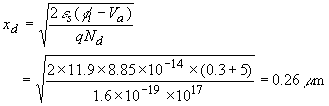
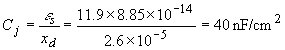
| Example 3.2 | Consider a chrome-silicon metal-semiconductor junction with Nd = 1017 cm-3. Calculate the depletion layer width, the electric field in the silicon at the metal-semiconductor interface, the potential across the semiconductor and the capacitance per unit area for an applied voltage of -5 V. |
| Solution | The depletion layer width equals:
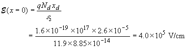
where the built-in potential was already calculated in Example 3.1. The electric field in the semiconductor at the interface is:
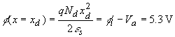
The potential equals:
And the capacitance per unit area is obtained from:
|
3.3.5. Schottky barrier lowering | |
Image charges build up in the metal electrode of a metal-semiconductor junction as carriers approach the metal-semiconductor interface. The potential associated with these charges reduces the effective barrier height. This barrier reduction tends to be rather small compared to the barrier height itself. Nevertheless this barrier reduction is of interest since it depends on the applied voltage and leads to a voltage dependence of the reverse bias current. Note that this barrier lowering is only experienced by a carrier while approaching the interface and will therefore not be noticeable in a capacitance-voltage measurement. |
An energy band diagram of an n-type silicon Schottky barrier including the barrier lowering is shown in Figure 3.3.2: |
| Figure 3.3.2: | Energy band diagram of a silicon Schottky barrier with φB = 0.8 V and Nd = 1019 cm-3. |
Shown is the energy band diagram obtained using the full-depletion approximation, the potential reduction experienced by electrons, which approach the interface and the resulting conduction band edge. A rounding of the conduction band edge can be observed at the metal-semiconductor interface as well as a reduction of the height of the barrier. |
The calculation of the barrier reduction assumes that the charge of an electron close to the metal-semiconductor interface attracts an opposite surface charge, which exactly balances the electron's charge so that the electric field surrounding the electron does not penetrate beyond this surface charge. The time to build-up the surface charge and the time to polarize the semiconductor around the moving electron are assumed to be much shorter than the transit time of the electron . This scenario is based on the assumption that there are no mobile or fixed charges around the electron as it approaches the metal-semiconductor interface. The electron and the induced surface charges are shown in Figure 3.3.3: |
| Figure 3.3.3: | a) Field lines and surface charges due to an electron in close proximity to a perfect conductor and b) the field lines and image charge of an electron. |
It can be shown that the electric field in the semiconductor is identical to that of the carrier itself and another carrier with opposite charge at equal distance but on the opposite side of the interface as shown in Figure 3.3.3 b). This charge is called the image charge. The difference between the actual surface charges and the image charge is that the fields in the metal are distinctly different. The image charge concept is justified on the basis that the electric field lines are perpendicular to the surface of a perfect conductor, so that, in the case of a flat interface, the mirror image of the field lines provides continuous field lines across the interface. |
The barrier lowering depends on the square root of the electric field at the interface and is calculated from: |
| (3.3.11) |
where |
Boulder, October 2007 |
 max is obtained from equation (3.3.10)